Design Summary
The design consists of two main subsystems: the data inputs and outputs and the processor. The following sections discuss each subsystem in depth and consider possible approaches to implementing the subsystem in the final design.
Data Input/Output
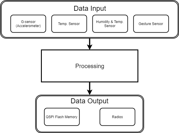
The data input and output subsystem is a basic part of our design. As its name implies, the data input/output subsystem manipulates the data transfer outside of the main processor and the co-processor. The input mostly handles data sent from the sensors and the output mainly writes the data into the flash memory or sends it to a radio which is outside of the FPGA board. This radio module is connected to the FPGA through the GPIO pins on the board.
For our design, there are three approaches/solutions based on the research we have conducted. We first considered the onboard FPGA sensors, because they are the most directly connected sensors. The direct connections are convenient for us to do some research and test its performance. For further study, considering the compatibility of our system, the other two solutions are a premade commercial daughter board/sensor array and a custom fabricated sensor array.

The quickest and most direct path forward for this subsystem is to simply use the onboard sensors provided by the chosen FPGA evaluation kit. These sensors will be most easily accessed and do not require purchasing, implementing or debugging any additional external hardware. The variety and resolution of the sensors available on the board are sufficient to our needs in proving our solution.
Utilizing a premade commercial daughter card containing a sensor array allows for greater flexibility in the chosen sensors for the design. This is desirable if a particular use case is identified that makes use of sensors not available on the DECA FPGA development board. The requirements are that the daughter card must be compatible with the FPGA and that an interface must be designed to facilitate the data transfer to the remainder of the design. This will add complexity to the project.
The most flexible and most complex solution is to use a custom fabricated sensor array. This would allow the team to select any sensor available for purchase, including sensors lacking daughter cards or other interfaces. This solution is complex because interfacing with the sensor would require a complete hardware interface design with the project. There will be little to no provided hardware support for the sensor array. In addition, this solution will add considerable development time.
Based on the increasing complexity and flexibility of each solution for subsystem 1, the design will initially be implemented with the on-board FPGA sensors. As the design matures, use-cases of the design will be identified, and if the use-cases require sensors that are not available on the FPGA, the design will be supplemented with the additional sensors. The team will first attempt to implement the sensors using a premade commercial daughter card sensor array, but if sensors are unavailable in that format, a custom fabricated sensor array will have to be implemented. This solution provides the maximum flexibility by allowing for the least complex sensor available to the device.
Processor Design
There are three approaches to implementing the main processor subsystem: Using a microcontroller such as the Arduino, using a commercial MSP430, or using a custom HDL implementation of the MSP430 processor.
An Arduino is a low-cost and easy to use microcontroller that would allow for rapid prototyping of sensors. The Arduino libraries include support for a large variety of sensor inputs and data outputs. Where the Arduino lacks, however, is in performing data transformations. The Arduino is an 8-bit microcontroller. This prevents it from handling large sets or values of data. It is also relatively slow and not necessarily optimized for every task of this project. Interactions with the hardware layer are all hidden behind a layer of abstraction, only accessible through simple libraries. This makes it easy to work with, as long as what is required is supported by the Arduino.
A commercial MSP430 provides a powerful, industry-standard device that would be able to handle the role of the main processor effectively. The MSP430 has been an industry standard microcontroller for years. Because of this, there are large amounts of support and help available online. Depending on the particular MSP430 board chosen, the MSP430 could bring a lot of extra board resources to the project that would not be utilized and could have a negative impact on the efficiency of the design. The largest drawback to using a commercial MSP430 is the lack of detailed control over the hardware. The project would have to utilize the MSP430 in its current form, and work around any difficulties, as correcting them is out of the scope of this project.

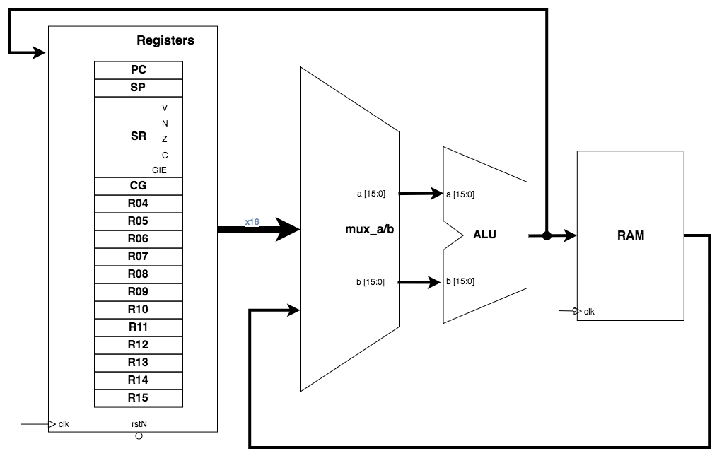
A custom HDL implementation of the MSP430 processor brings to the project all of the benefits of the previous solution, without the drawbacks. Because it is a custom HDL implementation, the team will have full control over the hardware and the integration into the other subsystems of the design. The major drawback this introduces is the responsibility to implement and ensure error-free functionality of the full MSP430 processor. This drawback is minimized within this project because the MSP430 HDL implementation has largely been completed. Figure 3 shows the architecture of the MSP430 CPU that is shared by the commercial MSP430 and the custom HDL MSP430. It depicts the 16 registers available to the MSP430, as well as the data flow between the registers and the RAM. Appendix A contains a complete MSP430 architecture block diagram, including control lines and addressing.
Based on the summaries of the benefits and drawbacks to the above solutions, the best choice forward for this project will be solution three. It provides the power and support of a full MSP430 while allowing for acute control of the hardware interactions with the remainder of the design.