Solution Methodology
The solution methodology will be split up into 5 main sections:
1. Key differences between a commercial STM and our STM
2. Tungsten tip
3. Piezoelectric disc
4. Transimpedance amplifier
5. Feedback loop
1. Commercial STM vs Capstone STM
Commercial STMs have four main differences in both solution and expectations in the form of piezoelectric material, control system, cost, and performance. The first figure illustrates what a piezo tube looks like and it is the main difference between a commercial STM and the capstone project. The capstone uses a 20mm piezo disc cut into four quadrants, which will be shown in section 3. The piezo tube is very rigid and requires 100s to 1000s of volts to move and scan a material vs the 5v we are using for our disc. This gives the commercial STM more granular control over their scan. The second big difference is the control system, our STM uses a software feedback loop or a hardware adder circuit whereas the commercial STM uses a proprietary solution with failsafes to ensure the safety of their hardware. The third difference is in the cost, our STM has a budget of $500 compared to the roughly $10,000 the commercial product costs. Lastly, overall performance is vastly different between the commercial product and our project. The second figure illustrates the best image we could find from a hobbyist STM (Dan Berard from dberard.com) and compared to the last picture form a commercial STM, the difference in quality is easy to see.
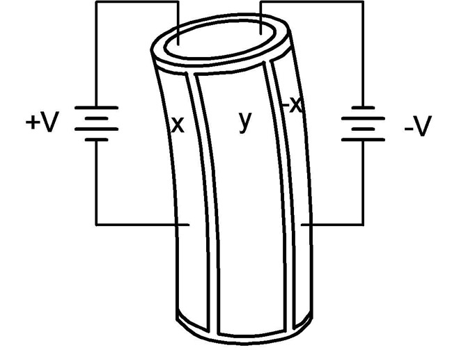
Figure 1: Piezoelectric Tube
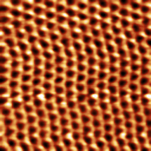
Figure 2: Hobbyist STM Image
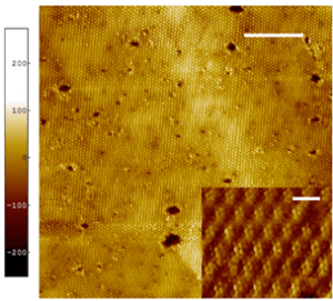
Figure 3: Commercial STM Image
2. Tungsten Tip
We need an atomically sharp conductive wire to accurately scan atoms, and we were able to chemically etch tungsten wire with sodium hydroxide to achieve this. This will enable atomic resolution for our scans. The steps on how we did this are outlined in the user manual in our final design report available in the documentation section, as well as the documentation document in our google drive. Figure 4 shows the sharpness of the tungsten wire under a microscope. Thank you to Ms. Madison King in the chemistry department for assistance and allowing us access to her lab!
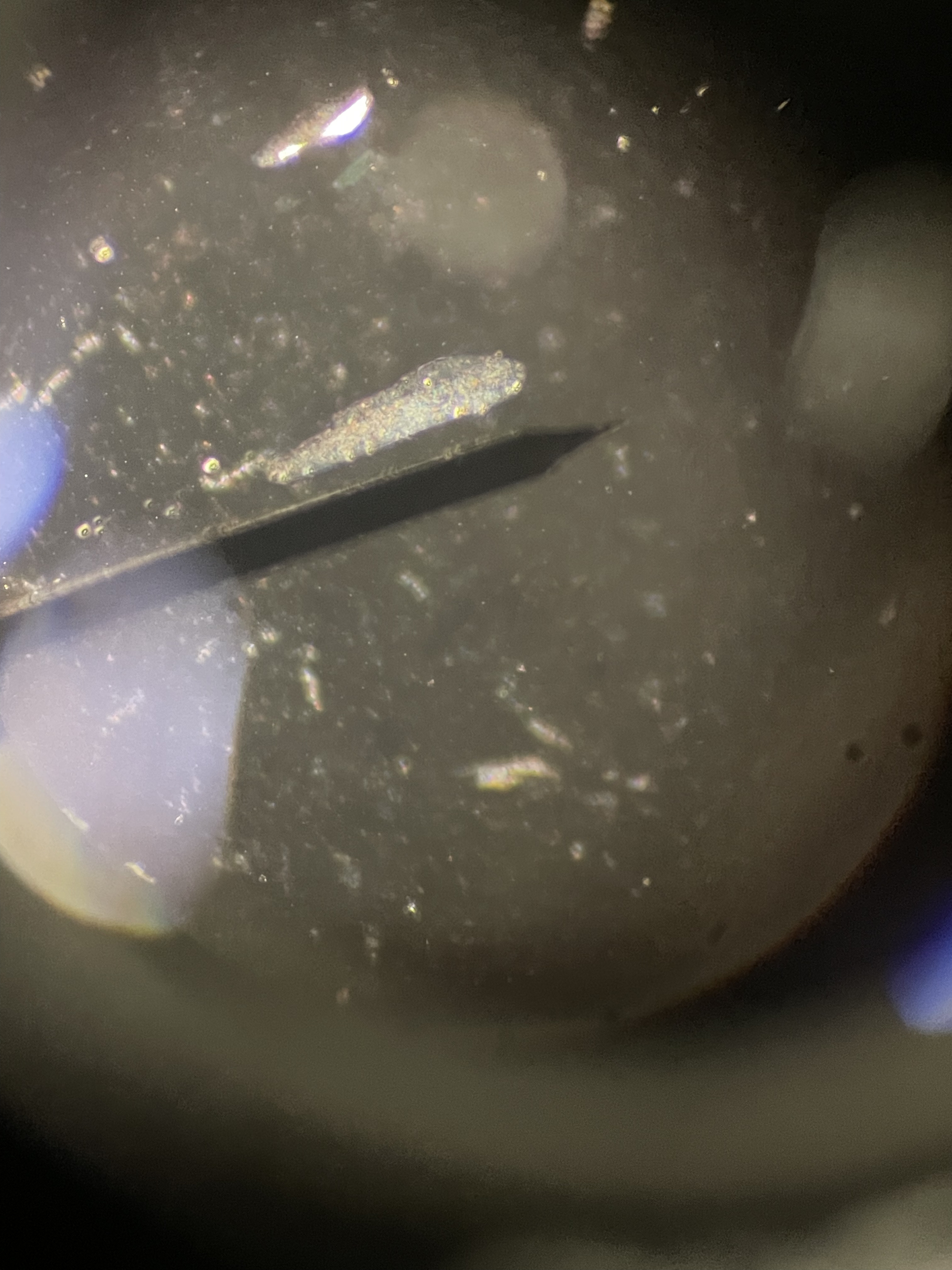
Figure 4: Tungten Tip
3. Piezoelectric Disc
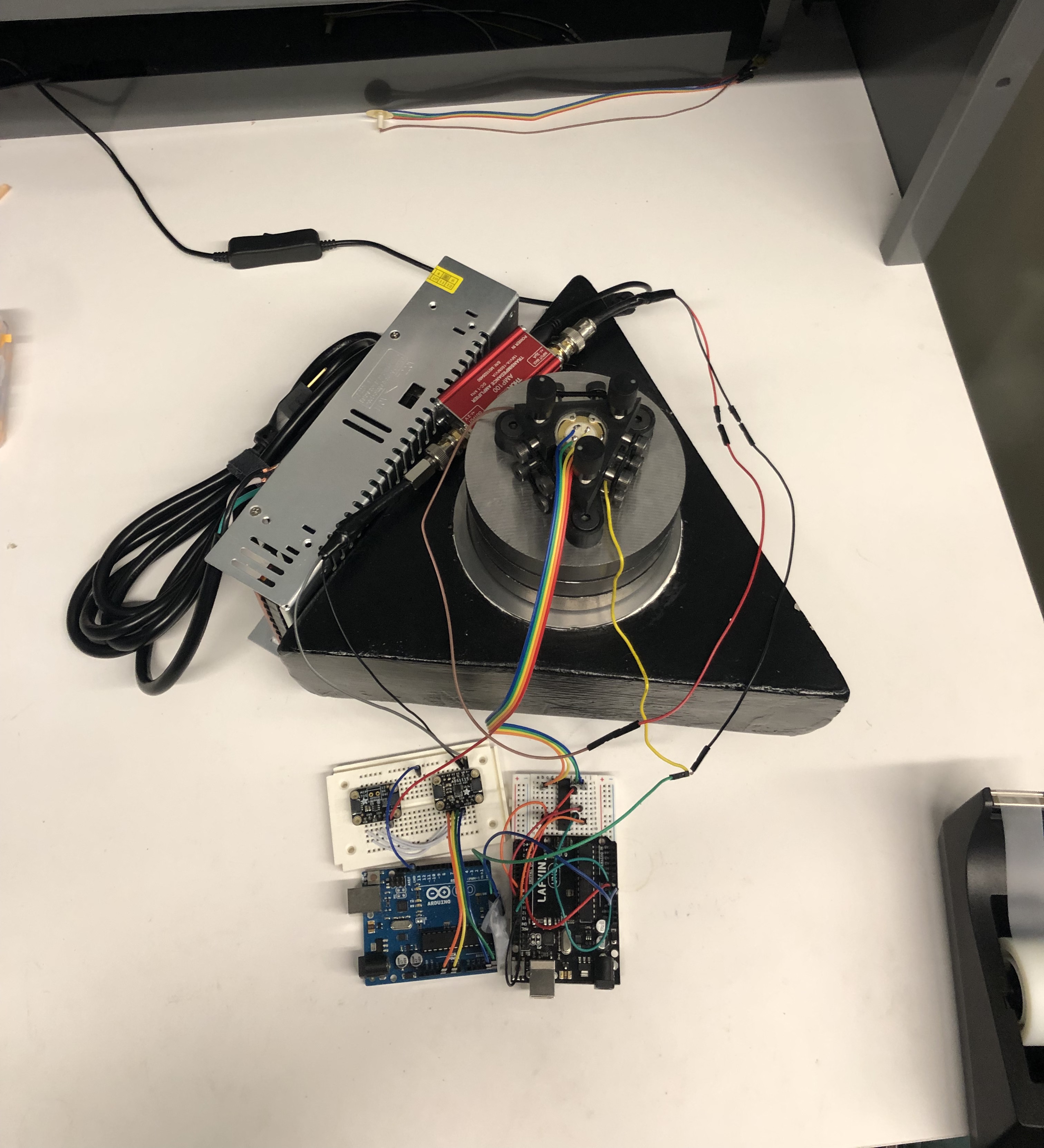
The piezoelectric disc is our main mechanism for scanning, and through cutting the disc into four quadrants we are able to control the X, Y, and Z axes. Our disc is also responsible for holding our scan assembly securly, ensuring we are able to get steady readings of the tunneling current between the tungsten tip and our material. Figure 5 illustrates the bend of the piezoelectric disc that occurs when applying a voltage which enables the scanning feature. Figure 6 shows our piezoelectric disc cut into four quadrants (+X, -X, +Y, -Y) and the wiring on each quadrant and the brass. Finally, figure 7 shows the final scan head assembly with the ceramic tip holder holding our tungsten tip.
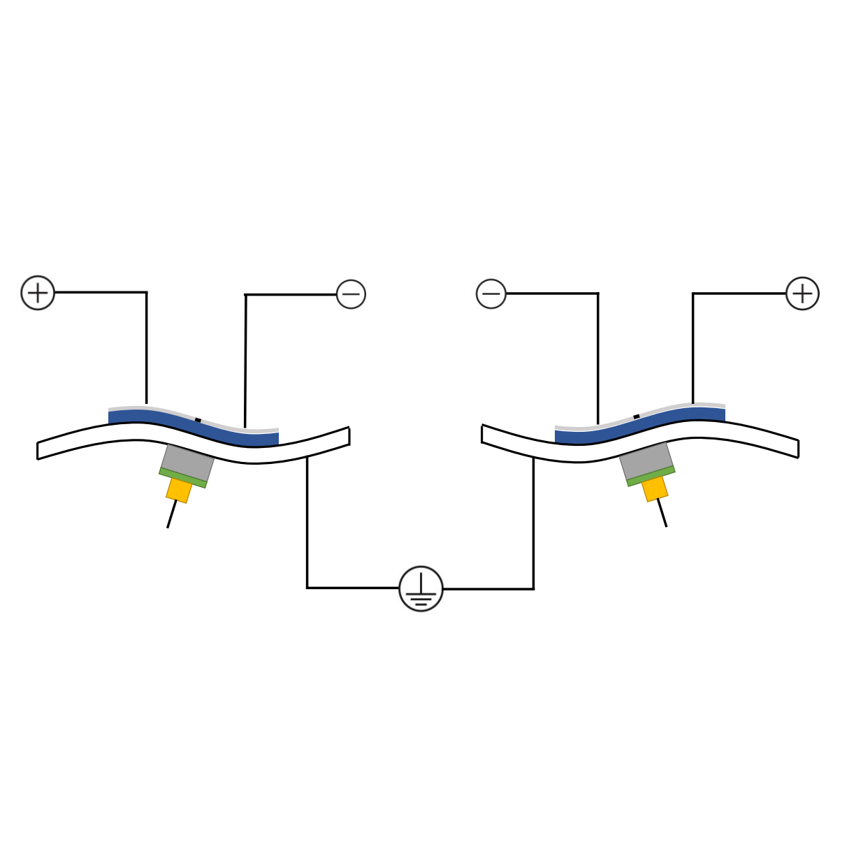
Figure 5: Piezo Disc Bend
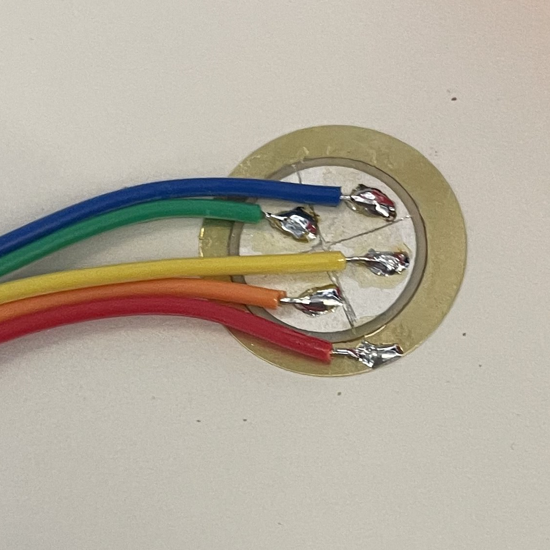
Figure 6: Piezo Disc Quadrants
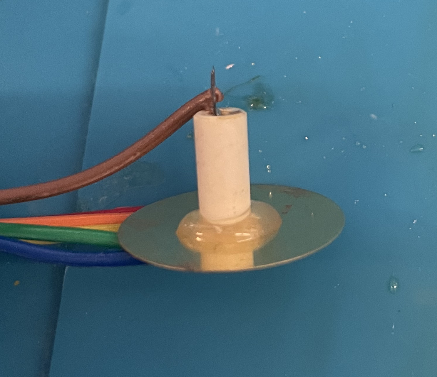
Figure 7: Scan Head Assembly
4. Transimpedance Amplifier
The tunneling current that we are expecting is in the range of nano amps, or 10^-9 amps which cannot be read through the Ariduino we are using. Because of this, we need a transimpedance amplifier to take in the tunneling current and output a voltage between 0-2 volts. Initially, we attempted to fabricate this circuit from scratch which ended up wasting a majority of our time. We ended up utilizing a commercial transimpedance amplifier from ThorLabs provided by our client, Dr. daCunha. It is shown in figure 8.
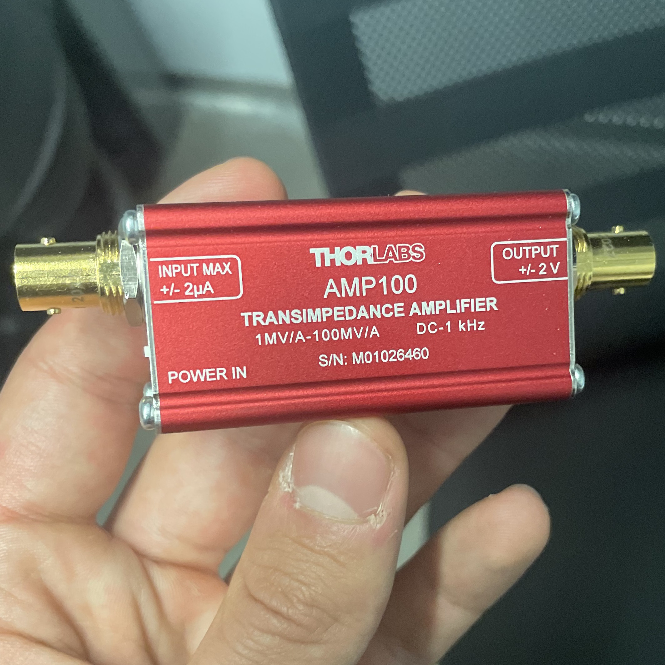
Figure 8: Transimpedance Amp from ThorLabs
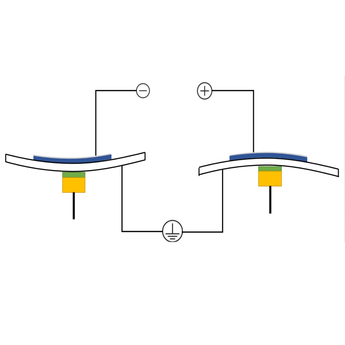
Figure 9: Z-Axis Bend
5. Feedback Loop
Through manipulation of the Z-Axis, we are able to implement a feedback loop to ensure we do not crash our tungsten wire into the material we are scanning which would result in bending, harming the resolution and sensitivity of our STM. Figure 9 demonstrates how we can bend the Z-Axis on the piezo disc. Our STM has gone back and forth between a hardware and software solution which trades the flexibility of code for the real time response and stability of hardware. Ultimately, we would suggest future teams to use a commercial solution to eliminate as many veriables and as much nosie as possible. Our code and schematics for the hardware feedback loop can be found in our final design report and the documentation document in our google drive.
Testing and Measurements
Testing and verifying our results proved to be very difficult since any noise we had was amplified and it was difficult to see if our tip was close to touching the material until it had already crashed. Through these obstacles, we were able to measure a constant output from our transimpedance amplifier of around 1.4V which is in the range between 0 and 2 volts. An image of our results are below:

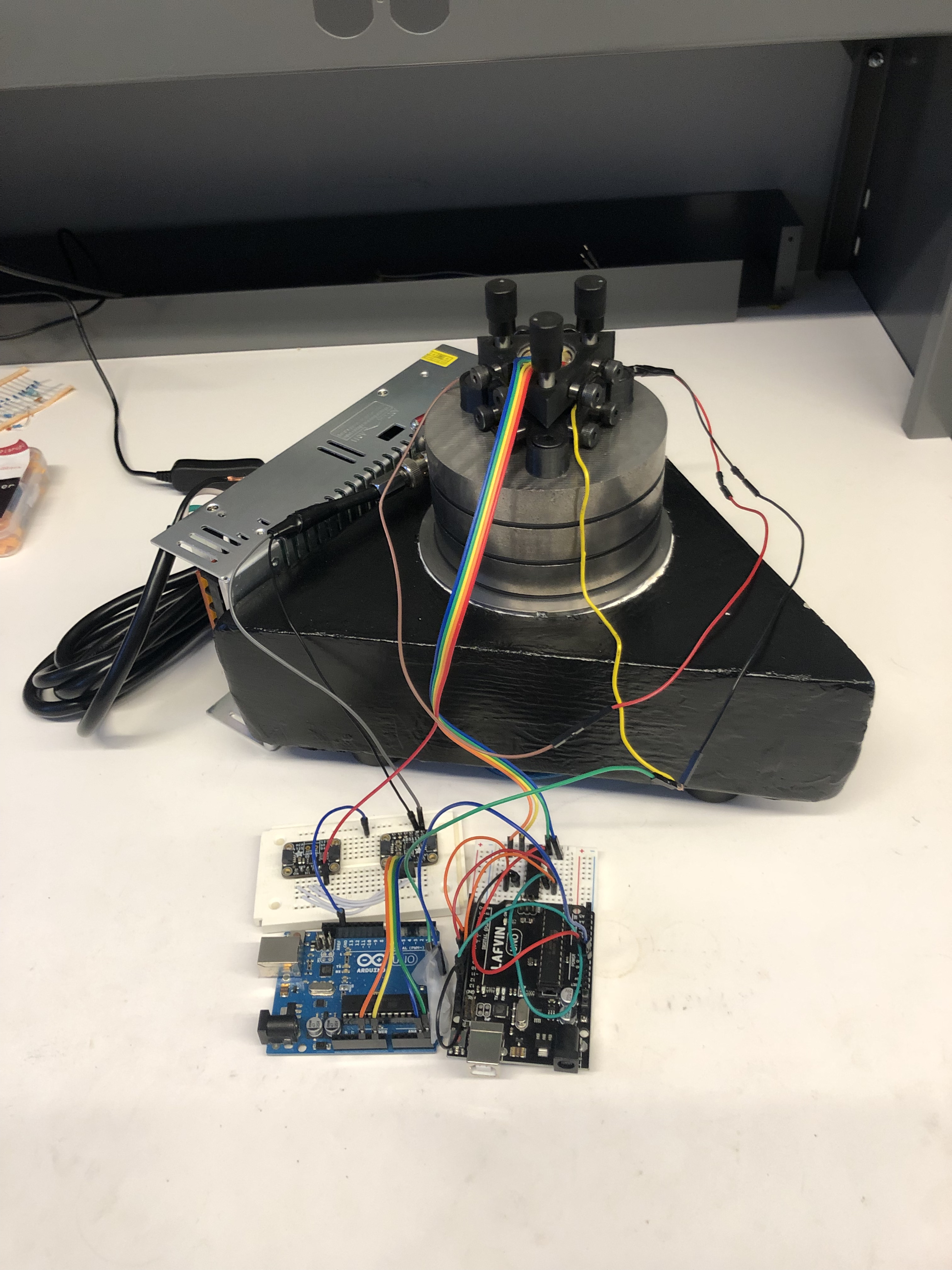
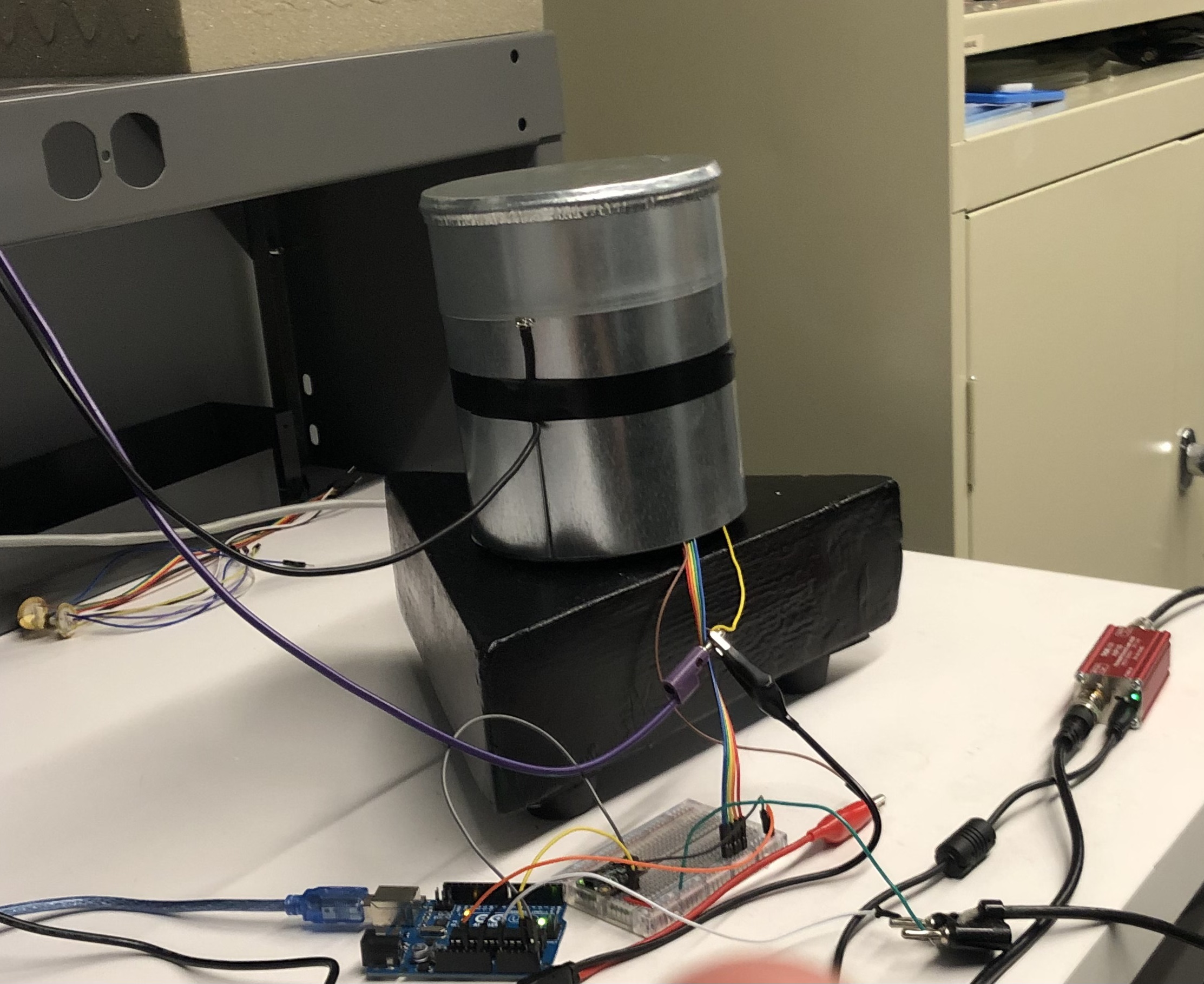
Three figures below are of the final version of our STM before we end off this semester:
