Space Radiation Detection Imaging System
NASA Team 2

Design Process: Phase 4


Key Milestones:


-- Sensor Board PCB Layout - 03/25/2015
-- Control Board PCB Layout - 04/05/2015
-- Final Presentation - 04/24/2015
-- Final Prototype Testing - ???
-- Final Client Report - 05/07/2015


PCB Layouts:


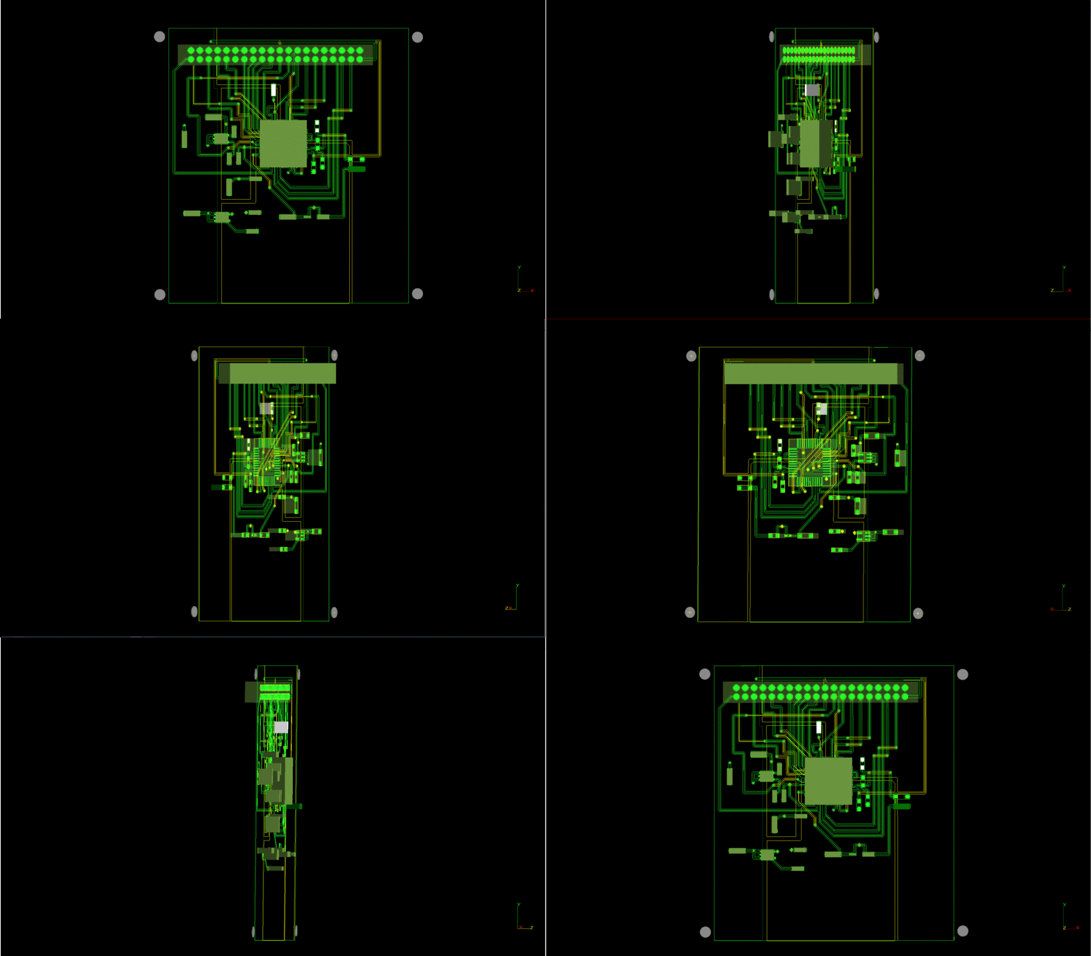
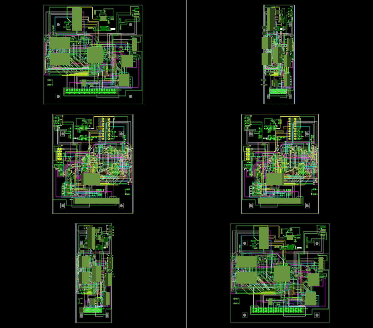
The team utilized the software, OrCAD PCB Designer, to create the physical layouts for the sensor board and the control board. This included creating the size of the board, indicating drill holes, adding appropriate layers, placing components, and routing traces appropriately. To verify that everything would fit onto the board, a parts-fit check was conducted using all the components in possession. After this design step was completed, NASA proceeded to fabricate both boards and mail them back to the team.

Sensor Board PCB Layout:
Control Board PCB Layout:

Final Prototype Testing:


Once both the sensor board and the control board were received, then testing could finally begin. The testing procedures were divided up as follows:

-- MATLAB Code Modifications
-- Sensor Board System Check
-- Control Board System Check
-- Picture Processing; Full System Check

The first step was to be certain that the MATLAB code did everything correctly in order to initialize the device, take pictures, and then send the data back to the host computer in a meaningful format. The next step was to verify the integrity of the sensor board which was done by connecting it to the old example model of the control board and observing if it was able to input and output data as expected. Afterwards, the control board had to be set up by first loading the CPLD with our AHDL code. At this point, the two boards were connected via the headers, and a full system test was started. This composed of positioning a camera lens in front of the CMOS sensor and taking a picture. If a discernible image was processed and sent back to the host computer, then the device would be considered fully functional.

Back