Space Radiation Detection Imaging System
NASA Team 2

Design Process: Phase 3
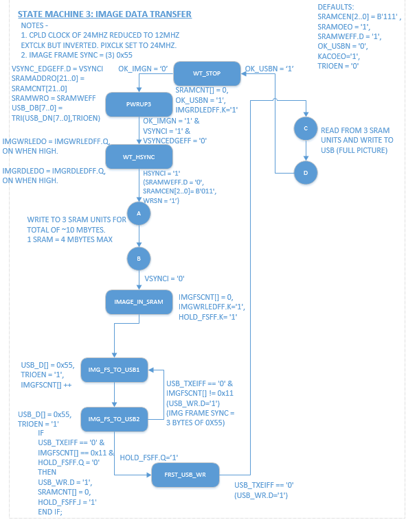

(State Machine Diagram 3)


Key Milestones:


-- State Machine Diagrams - 01/20/2015
-- Sensor Board Schematic - 02/11/2015
-- Control Board Schematic - 03/03/2015
-- Midterm Client Status Report - 03/08/2015
-- CPLD Simulations - 03/19/2015


State Machine Diagrams:


The figure to the left is an example of one of the three state machine diagrams that were created to map the signal behaviours in and out of the CPLD. This was an important first step to fully understand how all the components would communicate with each other.
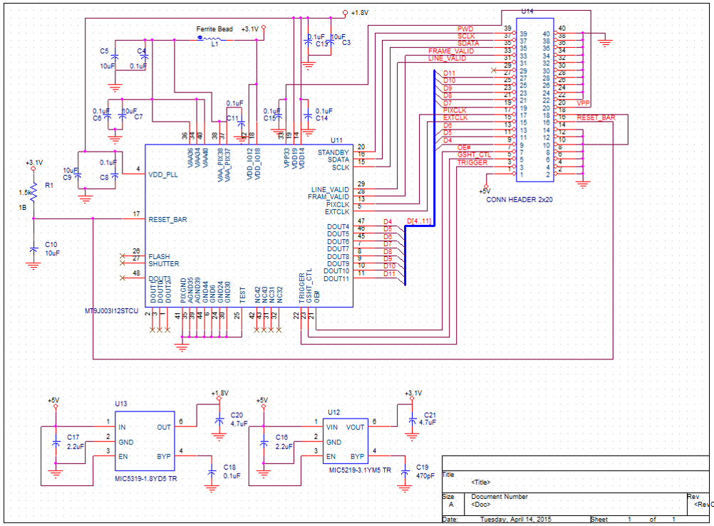

Schematics:


Our design is composed of two separate boards, the sensor board and the control board. The two boards are connected together by a 2x20 header. The sensor board comprises of the CMOS sensor, two voltage regulators, a header, a ferrite bead, and various capacitors and resistors. The control board contains the bulk of the components including the CPLD, SRAMs, I2C bus converter, USB adapter, oscillator, header, and other supporting parts.

Sensor Board Schematic:

Control Board Schematic:


CPLD Simulations:


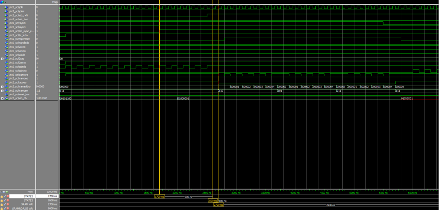
Initial signal simulations were carried out using the Altera Quartus application. This application allowed us to physically map out the pins of the CPLD and test the functionality of its AHDL code. To make sure that our state machine diagrams were being accurately followed, modifications had to be made to the AHDL code. Every possible path illustrated by the state machines had to be emulated by using the correct timings and inputs to observe the subsequent outputs. Once the simulation showed promise, the team could move on to starting the design of the PCB layouts.

Signal Timing Simulation:


Back