Space Radiation Detection Imaging System
NASA Team 2

Design Process: Phase 2


(Bill of Materials)


Key Milestones:


-- Comprehensive Components Research - 11/20/2014
-- Client Proposal - 12/05/2014


Parts Selection:


To the left is a list of all the essential components that the team anticipated will be needed for the design to function as desired. The overall calculated cost will be $193.55 which is within our target budget.

Key Components Specifications:


CMOS Sensor (MT9J003):

-- 10 MP Resolution
-- 1/2.3-inch Optical Format
-- 1.67x1.67 um Pixel Pitch
-- 6-48 MHz Input CLK
-- 1.7V - 3.1V Power Supply

USB Adapter (DLP-USB1232H):

-- USB 2.0 High Speed
-- USB to Parallel FIFO of 8 MB/s
-- 5V USB Power Supply
-- Uses FTDI's VCP or D2XX drivers

SRAM Memory (CY62177EV30):

-- 32M (2M x 16, 4M x 8) Size
-- 55ns Access Time
-- 2.2V - 3.7V Supply Voltage
-- Asynchronous Memory Type
-- Need Three to Store Image


I2C Bus Processor (PCA9564):

-- Parallel-Bus to I2C Bus Converter
-- 8 bits Parallel Data to Serial Data Stream
-- 2.3V - 3.6V Power Supply
-- 9 MHz Internal Oscillator for I2C Timing

CPLD (EPM3128ATC100-5):

-- 8 Logic Elements
-- 128 MacroCells
-- 98 I/0 Pins
-- 192.3 MHz Counter Speed
-- 3V - 3.6V Power Supply


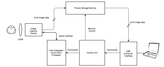
The picture below illustrates the basic design of the device. Commands initially flow from the host computer to the control unit (CPLD), where it determines to either send commands to the I2C processor or the Memory (SRAM). The I2C processor converts parallel data into serial data that the CMOS imager can understand. Once an image is captured, it is temporarily held in the SRAM until the computer is ready to receive it. This is done so that the device can take subsequent pictures without waiting for the computer to process the previous one.


General Design


Back